
Robohub.org
Chip design drastically reduces energy needed to compute with light
A new photonic chip design drastically reduces energy needed to compute with light, with simulations suggesting it could run optical neural networks 10 million times more efficiently than its electrical counterparts.
Image: courtesy of the researchers, edited by MIT News
By Rob Matheson
MIT researchers have developed a novel “photonic” chip that uses light instead of electricity — and consumes relatively little power in the process. The chip could be used to process massive neural networks millions of times more efficiently than today’s classical computers do.
Neural networks are machine-learning models that are widely used for such tasks as robotic object identification, natural language processing, drug development, medical imaging, and powering driverless cars. Novel optical neural networks, which use optical phenomena to accelerate computation, can run much faster and more efficiently than their electrical counterparts.
But as traditional and optical neural networks grow more complex, they eat up tons of power. To tackle that issue, researchers and major tech companies — including Google, IBM, and Tesla — have developed “AI accelerators,” specialized chips that improve the speed and efficiency of training and testing neural networks.
For electrical chips, including most AI accelerators, there is a theoretical minimum limit for energy consumption. Recently, MIT researchers have started developing photonic accelerators for optical neural networks. These chips perform orders of magnitude more efficiently, but they rely on some bulky optical components that limit their use to relatively small neural networks.
In a paper published in Physical Review X, MIT researchers describe a new photonic accelerator that uses more compact optical components and optical signal-processing techniques, to drastically reduce both power consumption and chip area. That allows the chip to scale to neural networks several orders of magnitude larger than its counterparts.
Simulated training of neural networks on the MNIST image-classification dataset suggest the accelerator can theoretically process neural networks more than 10 million times below the energy-consumption limit of traditional electrical-based accelerators and about 1,000 times below the limit of photonic accelerators. The researchers are now working on a prototype chip to experimentally prove the results.
“People are looking for technology that can compute beyond the fundamental limits of energy consumption,” says Ryan Hamerly, a postdoc in the Research Laboratory of Electronics. “Photonic accelerators are promising … but our motivation is to build a [photonic accelerator] that can scale up to large neural networks.”
Practical applications for such technologies include reducing energy consumption in data centers. “There’s a growing demand for data centers for running large neural networks, and it’s becoming increasingly computationally intractable as the demand grows,” says co-author Alexander Sludds, a graduate student in the Research Laboratory of Electronics. The aim is “to meet computational demand with neural network hardware … to address the bottleneck of energy consumption and latency.”
Joining Sludds and Hamerly on the paper are: co-author Liane Bernstein, an RLE graduate student; Marin Soljacic, an MIT professor of physics; and Dirk Englund, an MIT associate professor of electrical engineering and computer science, a researcher in RLE, and head of the Quantum Photonics Laboratory.
Compact design
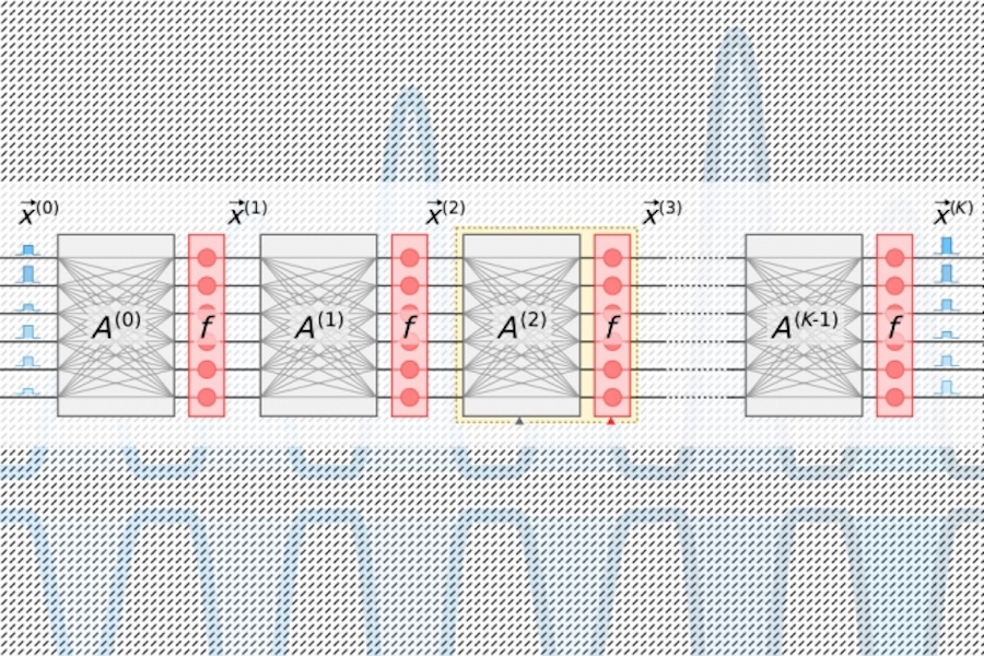
Neural networks process data through many computational layers containing interconnected nodes, called “neurons,” to find patterns in the data. Neurons receive input from their upstream neighbors and compute an output signal that is sent to neurons further downstream. Each input is also assigned a “weight,” a value based on its relative importance to all other inputs. As the data propagate “deeper” through layers, the network learns progressively more complex information. In the end, an output layer generates a prediction based on the calculations throughout the layers.
All AI accelerators aim to reduce the energy needed to process and move around data during a specific linear algebra step in neural networks, called “matrix multiplication.” There, neurons and weights are encoded into separate tables of rows and columns and then combined to calculate the outputs.
In traditional photonic accelerators, pulsed lasers encoded with information about each neuron in a layer flow into waveguides and through beam splitters. The resulting optical signals are fed into a grid of square optical components, called “Mach-Zehnder interferometers,” which are programmed to perform matrix multiplication. The interferometers, which are encoded with information about each weight, use signal-interference techniques that process the optical signals and weight values to compute an output for each neuron. But there’s a scaling issue: For each neuron there must be one waveguide and, for each weight, there must be one interferometer. Because the number of weights squares with the number of neurons, those interferometers take up a lot of real estate.
“You quickly realize the number of input neurons can never be larger than 100 or so, because you can’t fit that many components on the chip,” Hamerly says. “If your photonic accelerator can’t process more than 100 neurons per layer, then it makes it difficult to implement large neural networks into that architecture.”
The researchers’ chip relies on a more compact, energy efficient “optoelectronic” scheme that encodes data with optical signals, but uses “balanced homodyne detection” for matrix multiplication. That’s a technique that produces a measurable electrical signal after calculating the product of the amplitudes (wave heights) of two optical signals.
Pulses of light encoded with information about the input and output neurons for each neural network layer — which are needed to train the network — flow through a single channel. Separate pulses encoded with information of entire rows of weights in the matrix multiplication table flow through separate channels. Optical signals carrying the neuron and weight data fan out to grid of homodyne photodetectors. The photodetectors use the amplitude of the signals to compute an output value for each neuron. Each detector feeds an electrical output signal for each neuron into a modulator, which converts the signal back into a light pulse. That optical signal becomes the input for the next layer, and so on.
The design requires only one channel per input and output neuron, and only as many homodyne photodetectors as there are neurons, not weights. Because there are always far fewer neurons than weights, this saves significant space, so the chip is able to scale to neural networks with more than a million neurons per layer.
Finding the sweet spot
With photonic accelerators, there’s an unavoidable noise in the signal. The more light that’s fed into the chip, the less noise and greater the accuracy — but that gets to be pretty inefficient. Less input light increases efficiency but negatively impacts the neural network’s performance. But there’s a “sweet spot,” Bernstein says, that uses minimum optical power while maintaining accuracy.
That sweet spot for AI accelerators is measured in how many joules it takes to perform a single operation of multiplying two numbers — such as during matrix multiplication. Right now, traditional accelerators are measured in picojoules, or one-trillionth of a joule. Photonic accelerators measure in attojoules, which is a million times more efficient.
In their simulations, the researchers found their photonic accelerator could operate with sub-attojoule efficiency. “There’s some minimum optical power you can send in, before losing accuracy. The fundamental limit of our chip is a lot lower than traditional accelerators … and lower than other photonic accelerators,” Bernstein says.

AUAI is supported by: